UNIVERSITY of WASHINGTON | BOTHELL
Electrical Engineering | Science & Technology


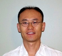
Seungkeun Choi, Ph.D.
Assistant Professor of Electrical Engineering
Science and Technology
University of Washington Bothell
Office: UWBB 228
Lab: UWBB 226
Email: schoi [at] uwb.edu
Phone: (425) 352-5437
Fax: (425) 352-3766
Brief Biosketch
Seungkeun Choi is currently an assistant professor in the Science and Technology Program at the University of Washington, located in Bothell, Washington, USA. His research interests range from the development of multidisciplinary sensors and actuators based on microelectromechanical systems (MEMS), to the design, fabrication and testing of light-weight flexible optoelectronics devices such as photovoltaics and light-emitting diodes.
He was born and raised in Seoul, Korea, and is a US permanent resident. He served in the military from 1991 to 1993. He studied at the Soongsil University in Seoul where he received a B.E. degree in Electrical Engineering in 1997. From 1997 to 1998 he was a semiconductor process engineer at the LG Semicon, Korea. He came to the State to attend the Pennsylvania State University in University Park, PA where he received M.S. in Electrical Engineering, specialized in image processing in 2000. He received the Ph.D. degree from the Georgia Institute of Technology, Atlanta, GA in 2007. For his Ph.D., he developed a low-power consuming resonant magnetic field sensor that can detect the direction of the Earth’s magnetic field. In 2007, he joined the Center for Organic Photonics and Electronics (COPE) in the same institute as a postdoctoral fellow where he developed large-area organic solar cells and light-emitting diodes. He published more than 15 peer reviewed journal articles and conference proceedings. He joined the faculty of the Science and Technology Program at the University of Washington at Bothell in 2012.
Education
Ph.D. in Electrical and Computer Engineering, May 2007
Georgia Institute of Technology, Atlanta, GA, USA
Dissertation: A Micromachined Magnetic Field Sensor for Low Power Electronic Compass Applications
Minor: Mechanical Engineering
Advisor: Prof. Mark G. Allen
M.S. in Electrical Engineering, August 2000
The Pennsylvania State University, University Park, PA, USA
Thesis: Robust Wavelet Image Coding with Packetization
Advisor: Prof. Nirmal K. Bose
B.E. in Electrical Engineering, February 1997
The Soongsil University, Seoul, Korea
Professional Experience
Adjunct Professor, August 2011 – May 2012
Southern Polytechnic State University, Electrical Engineering, Marietta, GA, USA
Postdoctoral Fellow, 2007 – 2012
Georgia Institute of Technology, School of Electrical and Computer Engineering Atlanta, GA, USA
Center for Organic Photonics and Electronics (COPE), 2007 - 2011
Institute for Electronics and Nanotechnolgoy (IEN), 2011 - 2012
Semiconductor Process Engineer, May 1997 – July 1998
LG Semicon (Hynix Semiconductor, Inc.), Manufacturing Technology Research Center Cheongju-si, Chungbuk, Korea
Military Service
Korean Army, April 1991 – November 1993
Experties
| Equipment | Atomic force microscope (Veeco AFM), Atomic layer deposition (ALD), Black magic PECVD (Carbon nanotube), DC/RF/Unifilm sputterer, E-beam evaporator, Filament evaporator, Lindberg furnace, Mask aligner (MA6), Obducat nanoimprint lithography system, Organic vapor deposition, Optical microscope, Plasma enhanced chemical vapor deposition (PECVD), Polisher, Profilometer, Reactive ion etching (RIE) machine, Scanning electron microscope (Zeiss SEM Ultra60), Signatone probe, Tousimis super critical dryer, Wirebonder, XPS (SSX-100). |
| Processes | Silicon oxidation (dry & wet), diffusion, silicon etching (ICP dry etching and KOH wet etching), photolithography (front and backside alignment), wafer bonding, Liftoff process, SiN and SiO2 deposition (RF sputterer and PECVD). |
| Devices | Devices: RF MEMS switch, Sensors and Actuators, Silicon resonators, Organic thin film transistors (OTFT), Organic photovoltaics (OPV), Organic light-emitting diodes (OLED), polysilicon-based photovoltaics. |
| Materials | Thin film metal-oxide (ZnO, IGZO, ITO, Al2O3), Organic semiconductors (pentacene, C60, P3HT:PCBM), Polymers (PEDOT:PSS, SU8, PMMA, PDMS), Thin film insulator (SiO2, SiN), Substrates (Glass, PES, PET, Silicon, Acrylic, Fused silica), Metals (Au, Ag, Cu, Ti, Cr, Ni, Al). |
Email: schoi [at] uwb.edu