Microfluidic Materials: Polymeric Laminate Technology
|
|
Microfluidic Materials: Polymeric Laminate Technology |
|
Materials and Fabrication
Microfluidic devices can be fabricated from a variety of materials. Based on fabrication techniques developed in the microelectronics industry, silicon has been used extensively to create microfluidic devices. In it's most basic form, the fabrication technique is as follows. A photoresist (positive or negative) is spun onto and silicon substrate. The photoresist is exposed to UV light through a high-resolution mask with the desired device patterns. After washing off the excess unpolymerized photoresist, the silicon wafer is placed in a wet chemical etching bath that anisotropically etches the silicon in locations not protected by photoresist. The result is a silicon wafer in which microchannels are etched. Often, a glass coverslip is used to fully enclose the channels and holes are drilled in the glass to allow fluidic access. For straighter edges and a deeper etch depth, deep reactive ion etching (DRIE) is an alternative to wet chemical etching. Silicon is an especially good material for microfluidic channels coupled with microelectronics or other microelectromechanical systems (MEMS). It also has good stiffness, allowing the formation of fairly rigid microstructures, which can be useful for dimensional stability.
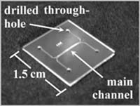
Figure 1. Photographic image of Si-Pyrex microdevice
(H-filter) used in the Yager laboratory. It consists of a Si
piece with anisotropically etched channels and four
mechanically drilled through-holes, covered by a Pyrex cover
that has been anodically bonded for a hermetic seal.
Another popular material for fabrication of microfluidic device is the silicone polymer, polydimethylsiloxane (PDMS). Microfluidic devices can be fabricated from PDMS by pouring the liquid form over a mold (usually silicon or photoresist) and curing to cross-link the polymer. The result is an optically clear, relatively flexible material that can be stacked onto other cured polymer slabs to form complex three-dimensional geometries. This cluster of techniques was developed in the laboratory of Prof. George Whitesides and has rapidly gained in popularity.
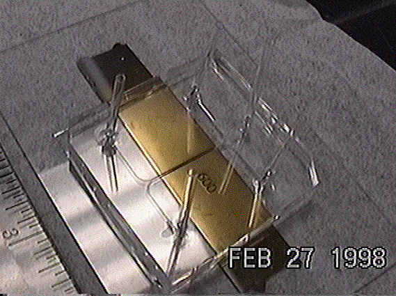
Figure 2. Photograph of a PDMS microfluidic device. It
consists of a flat glass plate onto which has been deposited
a gold layer in the form of two electrodes. The upper
portion of the device was formed by PDMS that was formed on
a mold that consisted of a flat Si surface that had been
etched to leave a ridge in the form a an H-filter (3 ports
in, 2 ports out). The 5 pieces of PDMS tubing used for
fluidic access was set into the device prior to curing. Note
that the clarity of PDMS makes it an excellent material for
microscopic observation of processes in the
microchannels.
Various plastics are also often used to fabricate microfluidic channels. For, example, hot embossing techniques can be used to imprint patterns into the surface of plastics, or injection molding may be used to create complex structures. Each of the techniques summarized below has its strengths and weaknesses.
Material: Fabrication Technique: Silicon Chemical wet etch Glass Chemical etch, laser cutting Polymeric films (e.g., Mylar) Laminate laser cutting Silicone elastomer (PDMS) Micromolding ("soft lithography") Photoresist, hydrogels, etc. Photopolymerization ("microfluidic tectonics") Thermoplastic Hot embossing, injection molding
This lab has adopted the technique developed in conjunction with Micronics, Inc. of Redmond of fabricating microfluidic devices from layered polymeric sheets. Outlines of the microfluidic device are cut in thin sheets of optically transparent Mylar with a CO2 laser cutting tool. The layers are bonded together with a thin adhesive layer to produce three-dimensional structures.
Figure 3. A schematic movie of how
polymeric laminates are stacked to produce three-dimensional
microfluidic devices and systems. The Julia set is purely
decorative. Movie in QuickTime format. If you are using a
Microsoft browser that no longer supports QuickTime, it's
not a problem I'm going to fix....
|
|
|
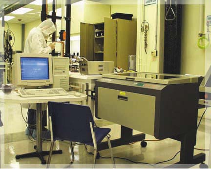
Figure 4. Image of the Universal Laser Systems CO2 cutting system as installed in the Washington Technology Center Microfabrication Laboratory at Fluke Hall. Many different graphics programs can use the printer drivers to control the cutting machine, which is approximately the size of a small office desk. |
This Universal Laser Systems CO2 laser cutting system allows conversion from CAD file to assembled polymeric laminate in hours.
![]()
Figure 5. Schematic of the mechanism that translates the focusing lens for the laser in the Universal Laser Systems cutter. The practical limit of feature sizes in Mylar we have found to be about 75 µm. This has proven adequate for most devices systems. Smaller features sizes can be achieved using other laser sources and other cutting methods.
Figure 6. Schematic of the process of assembly of
laser-cut polymeric parts. The most complex cut parts
consist of a carrier Mylar layer sandwiched by two layers of
pressure-sensitive adhesive. These two layers are, in turn,
capped by layers of siliconized release layers. The entire
5-layer sandwich is cut by the laser. The release layers are
removed, the cut parts aligned by assembly on a set of posts
that penetrate through-holes in the laminate, after which,
as shown at left, a cut or capping layer can be placed on
the first set of layers. Any bubbles trapped in the assembly
can be removed by pressing between rollers. This process can
repeated many times to create multilayer structures.
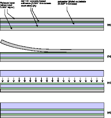
Figure 7. An example of the potential of the polymeric
laminate process to allow assembly of arbitrarily complex
microfluidic systems. The multiplicity of layers allows
crossover of channels, as well as the potential to use
different materials. Note that it is critical to design such
systems such that the adhesive layers do not face the
interior of the channels. However, it is not possible to
eliminate the adhesive from the edges of the channels--one
aspect of the method that leaves room for improvement. The
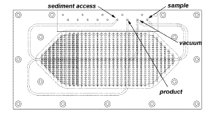
laminate a left was a design for a system for processing
water-based output from an air sampler to allow separation
of suspended particles by sedimentation rate while
continuously removing dissolved gases to prevent or remove
bubbles. The device is shown assembled below.
The most advantageous aspect of working with this system is the speed of the development cycle. There can be as little as 2-3 hours between the completion of a design using a CAD program and production of finished microfluidic devices of arbitrary complexity. This is a powerful new tool for rapid prototyping. Because it is also inexpensive, it is rapidly gaining in popularity at UW and elsewhere.
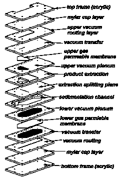
Figure 8. Schematic design of a complete flow
cytometry microfluidic system designed by Micronics, Inc.
The seven-layer laminate includes fluidic input ports and
waste storage chamber, valves, mixing structures,
observation ports, and a hydrodynamic focusing head to
create a focused stream of cells.
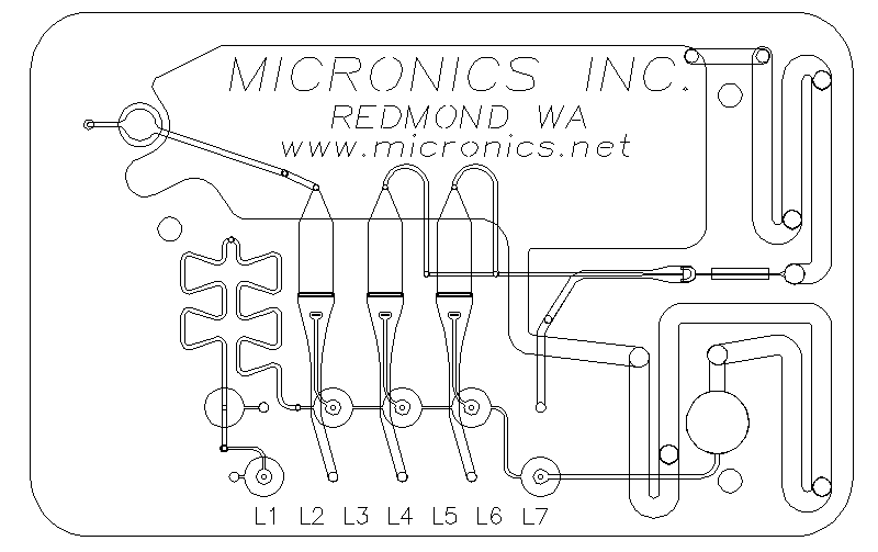
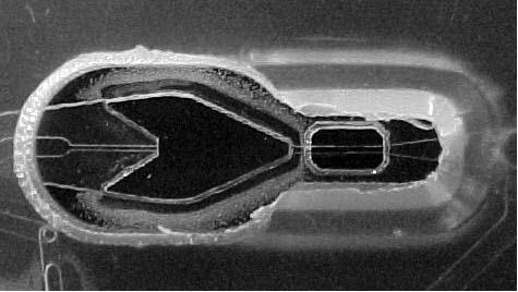
Figure 9. A flow cytometry hydrodynamic focusing
injector from Micronics, Inc. fabricated as a polymeric
laminate. It performs three-dimensional hydrodynamic
focusing. It is probed through an opening in the
injection-molded housing, and a Mylar window just right of
center.
Microfluidics to date (2001) has defied restriction to a single material--there are too may different types of applications for any one material or fabrication method to be adequate for all purposes. Polymeric laminate technology promises to one of the fabrication methods that will survive.
|
|
Return to Microfluidics Home Page Return to Yager Group Home Page
|