|
|
|
|
|
||
![]()
|
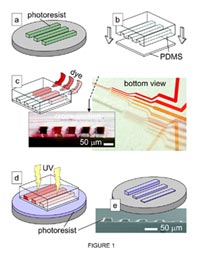
Novel photomasks make 3-D microstructures Scientists in the US have used a new technique to make complex, three-dimensional microstructures. Albert Folch and colleagues at the University of Washington in Seattle believe that their method could provide an inexpensive alternative to the traditional photolithographic approaches currently used to fabricate computer chips and other miniature structures (C Chen et al. 2003 Proc. Nat. Acad. Sci. to be published) In conventional photolithography a flat, patterned "photomask" is placed on top of a silicon wafer that has been coated with a light sensitive layer known as a "resist". Ultraviolet light is shone through the mask and exposes parts of the underlying material. Chemical etching then reveals the pattern created by the photomask. Light exposure is "all-or-none" and the process results in resist features of uniform height. The fabrication of three-dimensional structures thus requires several exposure steps, which is time-consuming and costly.
To overcome this "all-or-none" limitation, Folch and co-workers made a grey-scale photomask that allows differing amounts of light to pass through it. The photomask is made from a polymer that is transparent to ultraviolet light and contains light absorbing dyes. The concentrations of dye can be varied to allow more or less light through the system, which allows the researchers to accurately "sculpt" a three-dimensional resist surface. A variety of complex shapes with varying heights - such as "wedges" and "staircases" - can be formed in a few seconds. "The advantage of the technique is that it allows for an arbitrary number of grey-scales," Folch told PhysicsWeb. Previous approaches could only manage a few grey-scale levels. Although the method has not been optimized, the team believes that the photomasks could be used in a wide variety of applications in addition to the fabrication of computer chips. These include microoptic elements, tissue-engineering scaffolds and other biotechnological applications. "We are interested in combining these devices with live cells," Folch added. "The photomasks are particularly suited for cellular applications because the polymer from which they are made is biocompatible." Author
|
|
||||||||||||||||||||||||||||||||||||||||||||||||||||||||||||||||||||||||||||||||||||||||||||||||||||||||||||||||||||||||||||||||||||||||||||||||||||||||||||||||||||||||||||||||||||||||||||||||||||||||||||||||||||||||

|
||||||||||||||||||||||||||||||||||||||||||||||||||||||||||||||||||||||||||||||||||||||||||||||||||||||||||||||||||||||||||||||||||||||||||||||||||||||||||||||||||||||||||||||||||||||||||||||||||||||||||||||||||||||||||
Home |
News | Physics World | PhysicsJobs | Resources | Events | Best of PhysicsWeb
Tel +44 (0)117 929 7481 | Fax +44 (0)117 925 1942 | E-mail info@physicsweb.org |
||||||||||||||||||||||||||||||||||||||||||||||||||||||||||||||||||||||||||||||||||||||||||||||||||||||||||||||||||||||||||||||||||||||||||||||||||||||||||||||||||||||||||||||||||||||||||||||||||||||||||||||||||||||||||